PCB Manufacturing
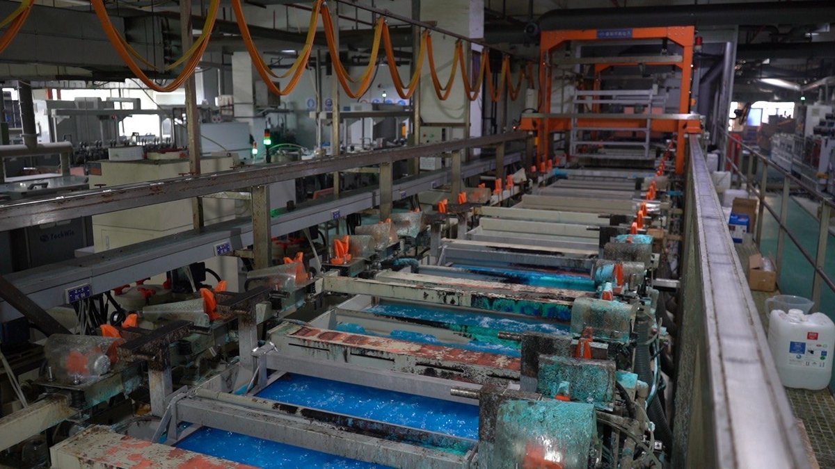
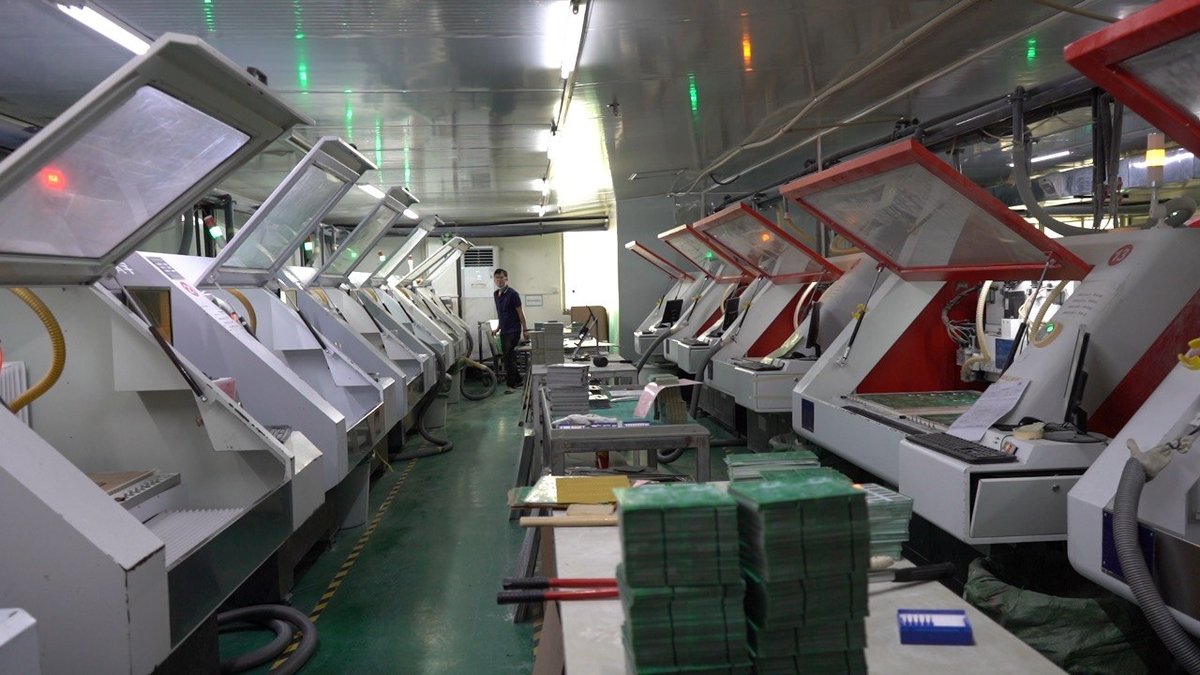
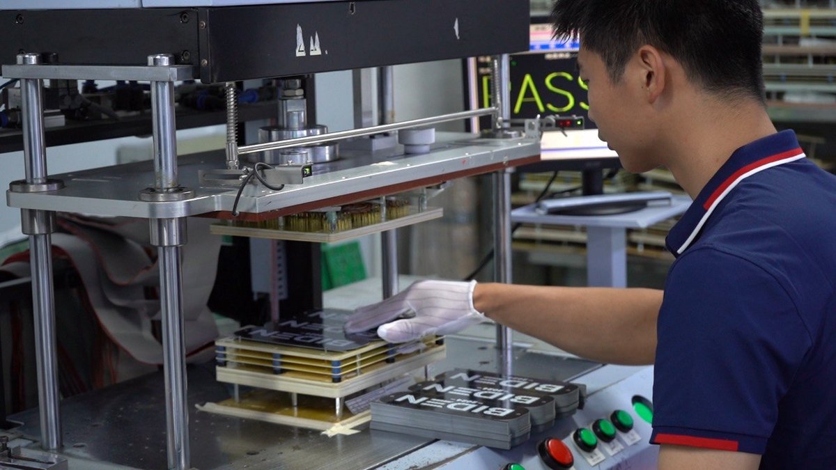
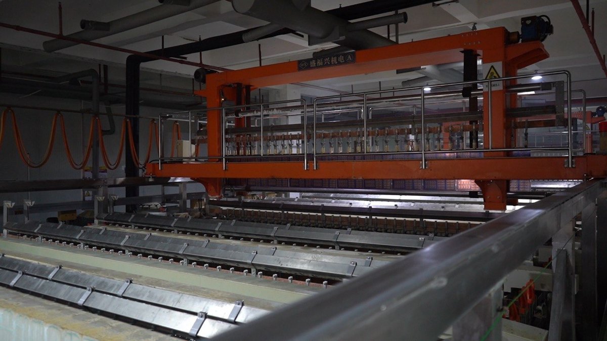
PCB Manufacturing Process
From raw laminate to finished PCB — full in-house production capabilities
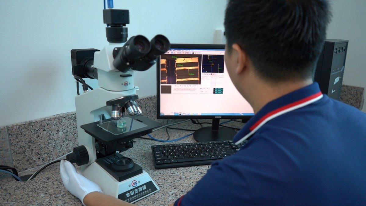
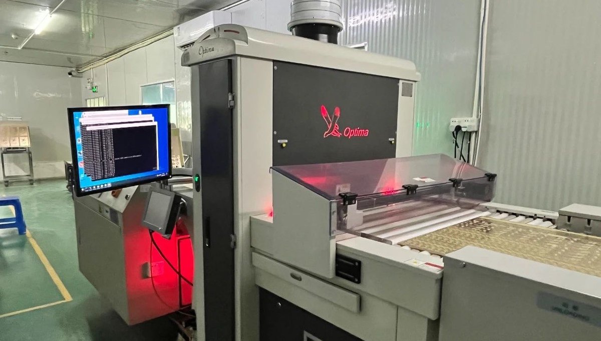
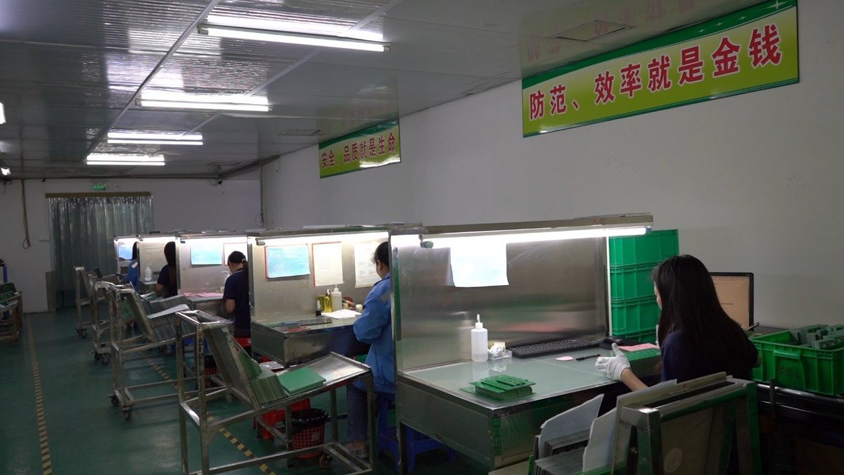
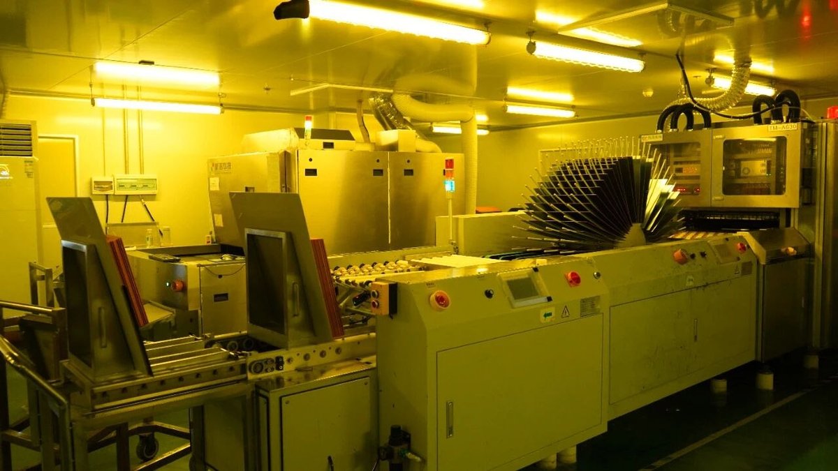
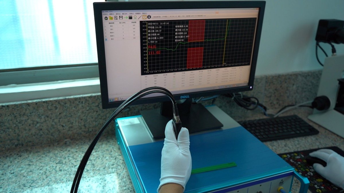
High Density Interconnect
- Max Layers24L
- Min Line/Space3mil
- HDI Any-layer3rd Order
- Blind & Buried ViasSupported
Precision & Speed
- Min Laser Drill0.10mm
- Impedance Tolerance±10%
- Prototype Lead Time3 Days
- Small Batch5 Days
Reliability & Quality
- Defect Rate<0.1%
- Warpage Control≤0.75%
- AOI + E-Test100% Inspected
- IPC Class2 / 3
Versatility
- Heavy CopperUp to 12OZ
- Max Board Size600×400mm
- Surface FinishENIG / HASL / OSP
- Solder Mask Colors6 Colors
Download Full Capability Specs (PDF)
34 detailed process parameters · Updated April 2026
PCBA Assembly
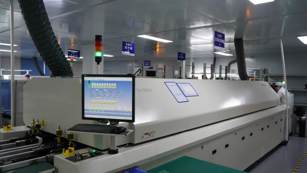
PCBA Assembly Process
Complete SMT + THT assembly, testing and inspection in-house
| Category | Capability | Details |
|---|---|---|
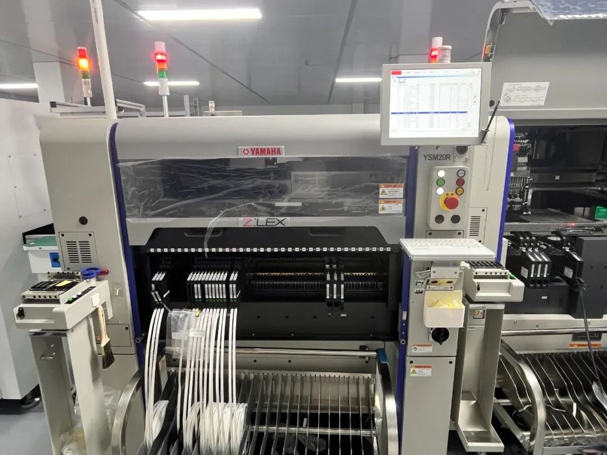
| Assembly Speed | 4M+ points/day | SMT high-speed line |
| Min Component | 01005 (0.4×0.2mm) | Fine-pitch supported |
| Mounting Accuracy | ±0.0375mm | Yamaha YS20 precision |
| BGA Pitch | 0.25mm min | QFN / BGA / LGA |
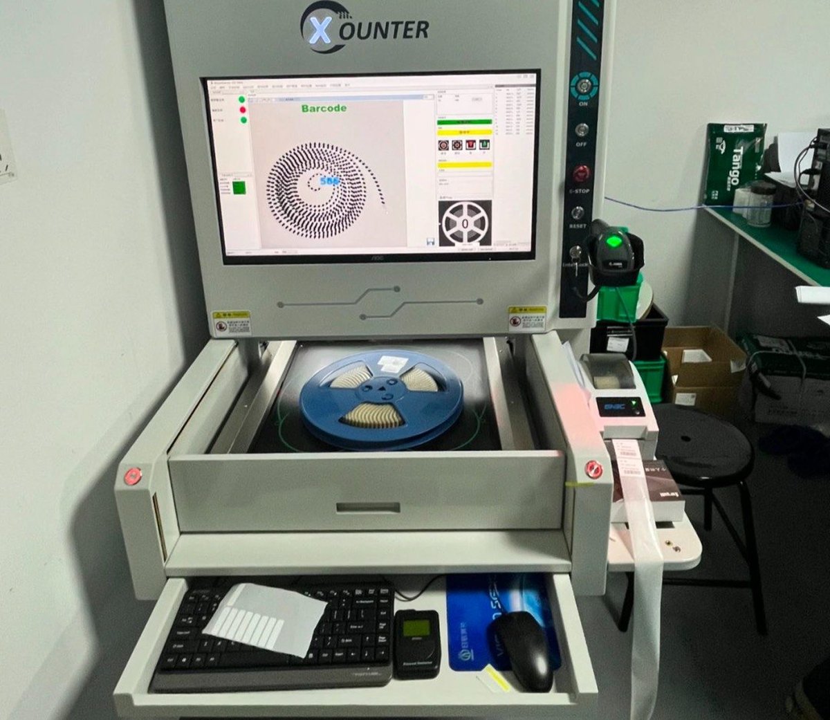
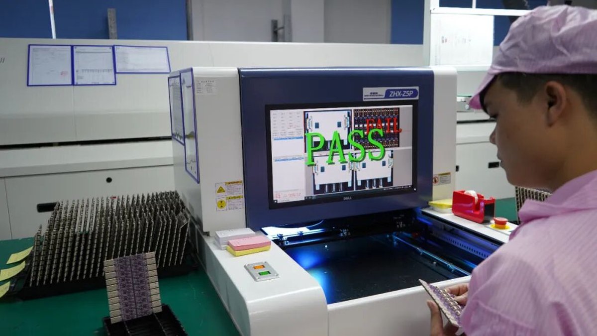
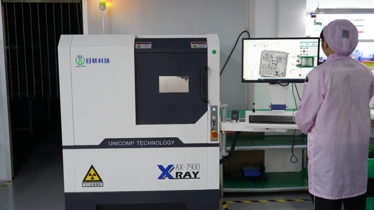
| Inspection | 3D AOI + X-Ray | 100% coverage, BGA hidden solder |
| Testing | ICT + FCT | Flying probe + custom fixtures |
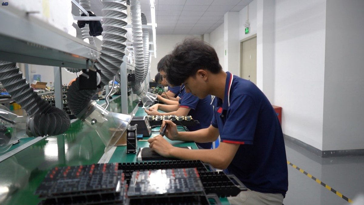
| Services | SMT + THT + Box Build | One-stop turnkey |
| Programming | MCU / Flash / EEPROM | In-house programming |
| Min Order | 1 Set | Prototype to mass production |
| RoHS | Lead-Free available | RoHS / REACH compliant |
From Prototype to Mass Production
ISO 9001:2015 · RoHS Compliant · Full In-House Production
Contact Us →